D'Flux PCB Desoldering Workstation (Thesis Project)
August '18 - July '19
I did Industrial design and Design Research with one project partner under the guidance of a professor. The problem was to design for segregation stage in e-waste management by easy, quick and safe dismantling of Printed Circuit Boards.
We worked on the project using the Creative Engineering Design Process and built a 1:1 scale working prototype of the PCB De-soldering Workstation. I did research, user interviews, empathy and literature study in the initial stage of design, CAD modeling, resin prototyping and sheet metal manufacturing in the building phase of the design.
Fusion 360 and AutoCAD for CAD are some software used. We referred to online journals and academic papers from our department library to understand the problem of e-waste and pin-point to the problem of designing a workstation for workers who dismantle PCB.
Process
01 User Research
02 Problem Identification
03 Ideation
04 Concepts
05 Test Rig
06 Prototype
User Research
First, we were assigned to solve the problem of garbage segregation. The management of waste product is a wide and complex task which is currently done manually in India. Workers working in unsanitary and unsafe conditions is common sight in waste management. While, we delved into the subject of waste, we came across a fairly ignored category of e-waste.
E-waste is the result of disposal of electronics, the need for electronics is essential though disposal is usually neglected. We identified the workers and small enterprises that deal with disposal of e-waste and found shocking methods used to dispose off Printed Circuit Boards. We found that main reason for employing people instead of machines is the cost of the machines themselves, so we approached the problem by looking at the steps used by a worker to dismantle PCB:
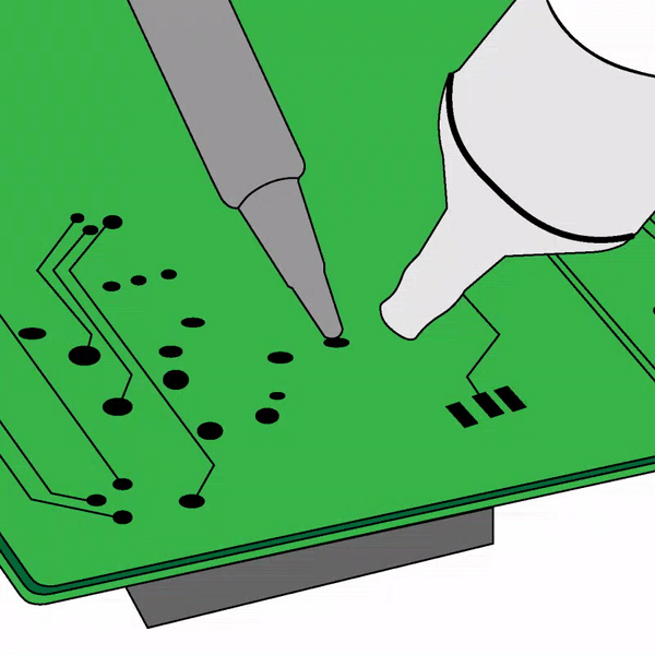
1. Desoldering of components by openly heating PCB. It releases toxic fumes.
2. Chemical etching to remove copper layer.
3. Chemical(Hard Acid) wash of components to deposit gold plate connectors.
4. Stripping of wires for copper.
5. Crushing of plastic parts.
6. Segregation of ferrous and non ferrous materials.
7.Separation of aluminum through eddy current.
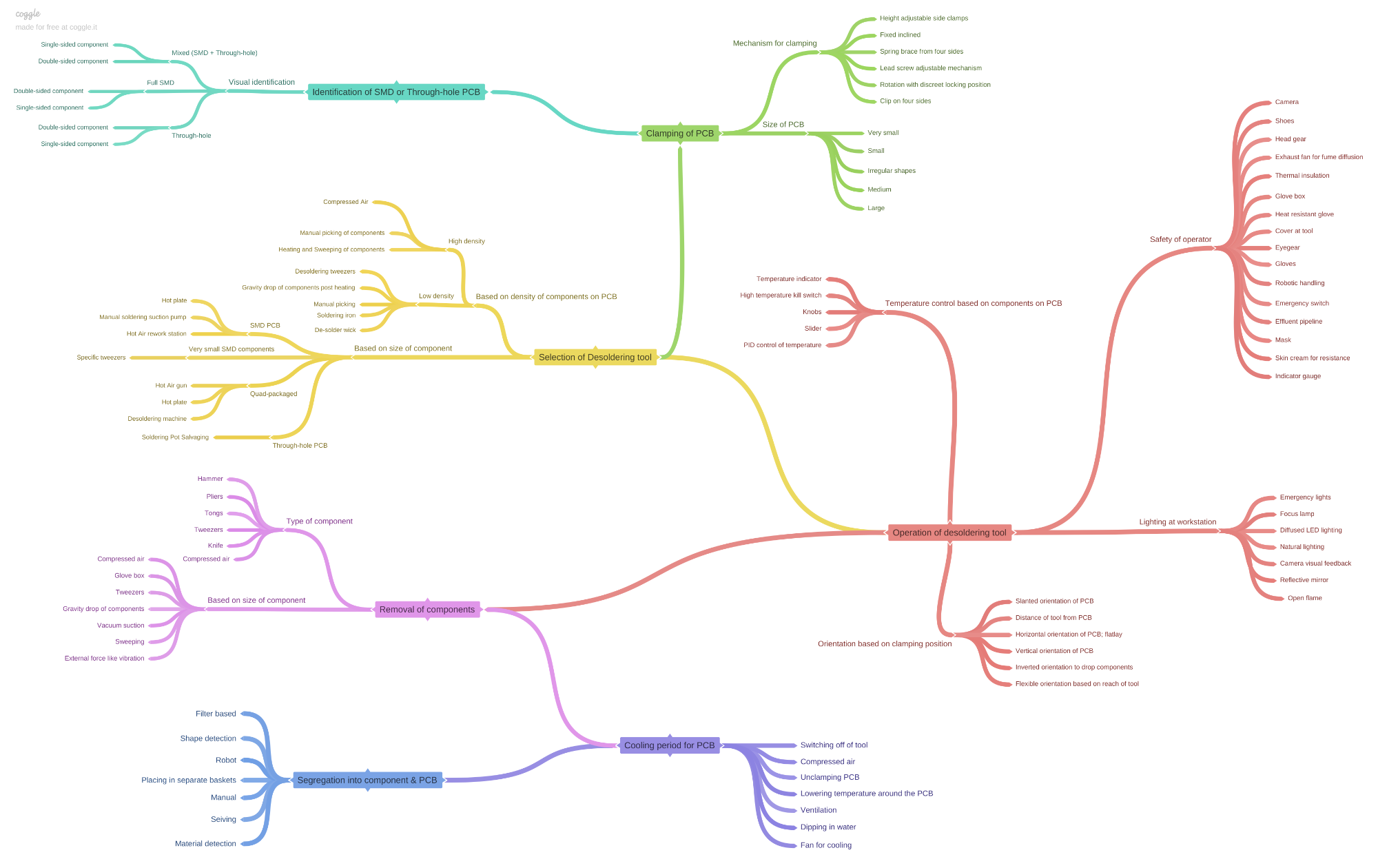
Problem Identification
We followed the Creative Engineering Design Process to do an Innovation Situation Questionnaire for analysing the problem into sub-systems and found a list of Preliminary Requirements for our product:
1. Holding the PCB
2. Visibility of task of removing components
3. Proper Lighting of workspace
4. Easy removal of solder
5. Easy removal of components
6. Less time required per job
7. Protection from heat, toxic fumes and chemicals
8. Storage for components and PCB
9. Low cost
Ideation
We did brainstorming for ways to solve each task involved in dismantling of PCB through manual effort and studied each desoldering technique for removal of PCB components.
Concepts
We generated an array of concepts and selected the most feasible of all the concepts.
Below is a few concepts which we sketched:
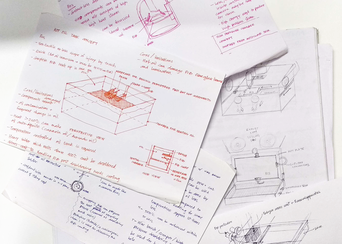
We selected a concept by using the weighted matrix method of selection which was the most feasible of the options to build within our deadline.
Below is the CAD model of our final selected concept:
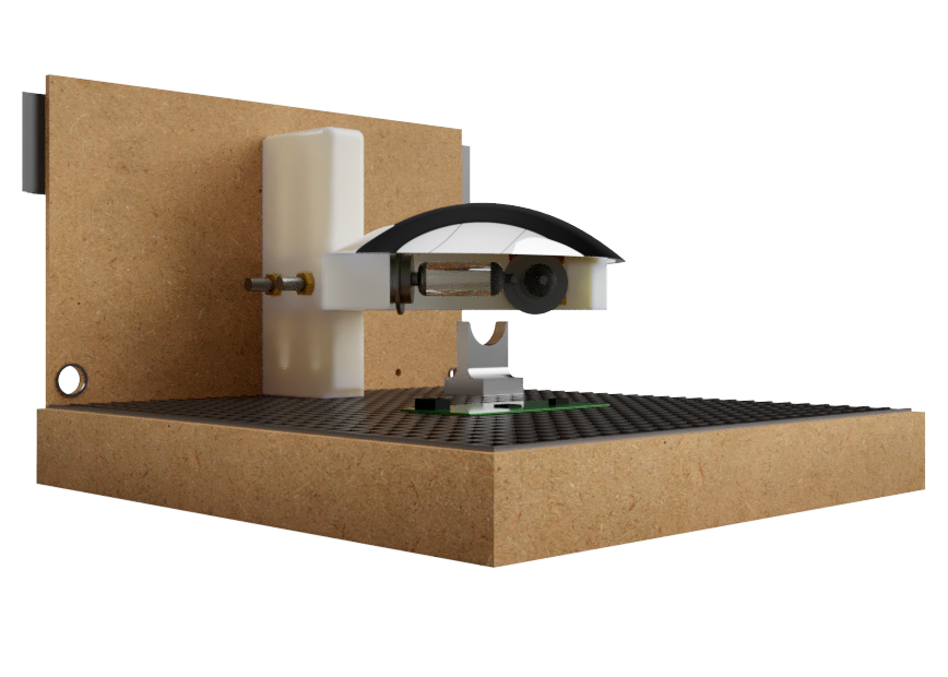
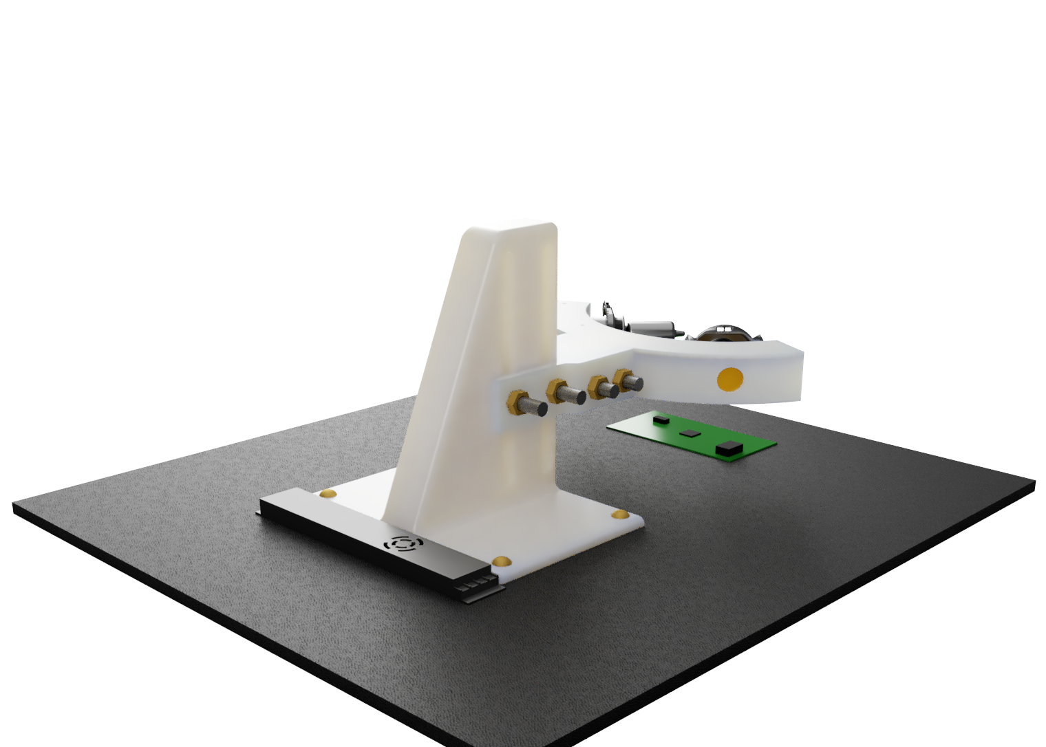
Test Rig
We built a test rig after 3D modeling the concept on Fusion 360 and 3D printed it to test the effectiveness of the method for dismantling PCB.
Below is a CAD render of our test rig:
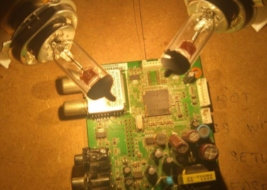
Below is the testing of our concept:
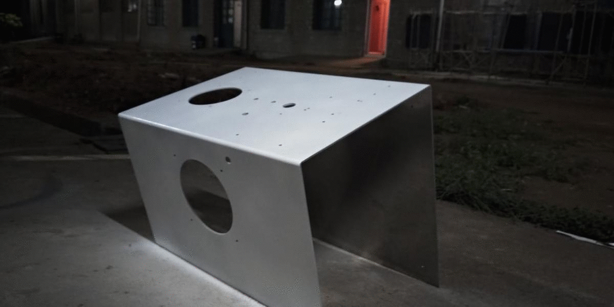
Prototype
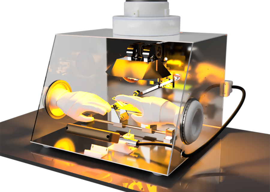
We prototyped our product using MS sheets, acrylic, resin epoxy and ABS 3D printed internal components. We used Arduino Mega, 100/130W Halogen lamps, thermocouple, 12000 RPM DC motor as components to build the prototype.
Below is the CAD model of our final prototype:
Below are some snapshots from prototyping: